
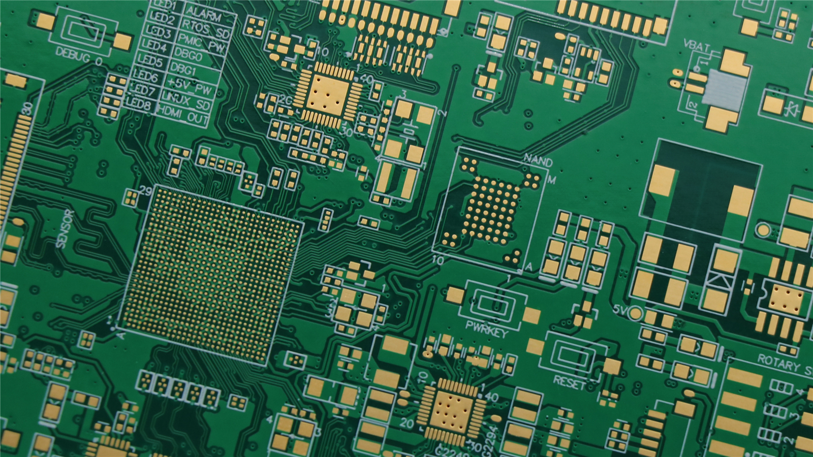
HDI
(76 reviews)
HDI
HDI PCB
High Density Interconnect boards with microvias for miniaturized high-performance devices
Key Features
Microvias
Laser drilled ≤0.15mm
High Density
Fine pitch components
Any Layer HDI
Advanced interconnect
Via-in-Pad
Maximum routing density
Specifications
| Via Size | 0.05mm - 0.15mm |
| Layer Count | Up to 20+ layers |
| Min Trace | 0.075mm (3mil) |
| Build-up | 1+N+1 to 4+N+4 |
| Applications | Smartphones, Tablets, IoT |
Engineering considerations
Manufacturing review before quote
HDI boards need fabrication and assembly decisions to stay linked. A realistic stackup and via strategy should be reviewed before the layout is frozen.
- Confirm layer count, microvia structure, sequential lamination, via-in-pad requirements, and the escape strategy around fine-pitch packages.
- Review stackup, impedance-sensitive layers, copper balance, registration, solder mask, and inspection access before release.
- Align the fabrication build with BGA assembly, X-ray or AOI coverage, test access, and the product reliability stage.
Typical applications
Smartphones, Tablets, IoT