Impedance Control
3 articles
More Impedance Control articles
Additional related articles that still fit the manufacturing topic cluster but are not part of the featured editorial grouping.
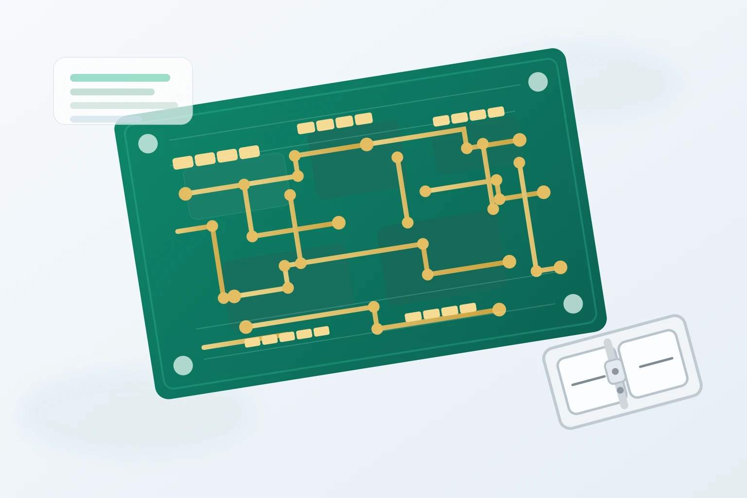
PCB Stackup Design Guide: How to Plan Layers, Reference Planes, and Manufacturing Constraints
This practical PCB stackup design guide explains how to assign signal and plane layers, choose materials and thickness assumptions early, and send a clearer stackup package for fabrication or PCBA feedback.
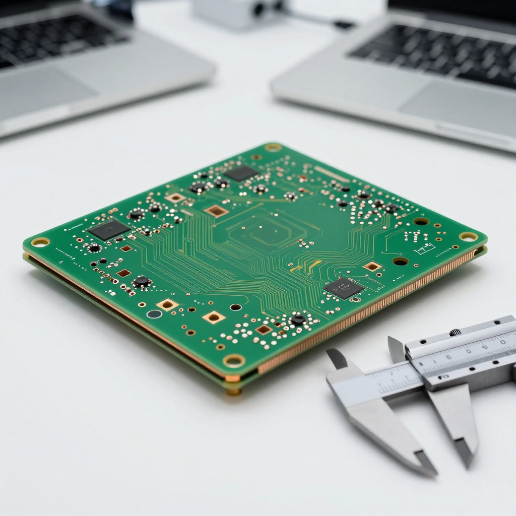
Controlled Impedance PCB Design Guide: Stackup, Trace Geometry, and Manufacturing Handoff
Controlled impedance PCB design depends on more than a calculator result. This guide covers stackup planning, trace geometry, material assumptions, fabrication notes, and the handoff details that help PCB manufacturers quote and build signal-sensitive boards with fewer surprises.
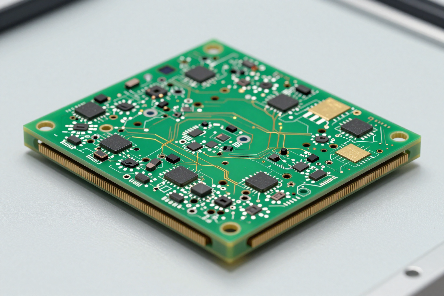
Multilayer PCB Design Guide: Stackup Planning, Layer Count, and Manufacturing Tradeoffs
This practical multilayer PCB design guide explains when extra layers are worth adding, how to plan stackup and return paths, what via and escape routing tradeoffs matter, and how to send a cleaner package to your PCB manufacturer.